
Overview
Class A/B amplifiers are the most common amplifier topology found in car audio. Understanding how they work, including their transistor pairs, dual voltage rails, signal path, and efficiency characteristics, helps explain both their strengths and their limitations. This article covers the fundamental operating principles of a classic Class A/B design, including how biasing is set to eliminate crossover distortion.
Voltage Rails: Single vs. Dual Supply
A basic amplifier may operate from a single positive supply rail, but a classic Class A/B design uses dual voltage rails: one positive and one negative (for example, +12 V and -12 V). Together, these two rails provide a full 24 V of voltage swing for the output stage.
This dual-rail arrangement is important because it allows the amplifier output to swing both above and below ground (0 V) without requiring a large output coupling capacitor to block DC, though some designs still include one at the output for protection.
Signal Path: From Source to Speaker
1. Common Ground Reference
All major components share a common ground bus: the negative supply rail, the positive supply rail return, the signal source (e.g., a phone or head unit), and the speaker return. This shared reference is fundamental to how the circuit operates.
2. Input Coupling Capacitors
The audio signal from the source enters through input coupling capacitors. These capacitors block any DC offset present on the source output and pass only the AC audio waveform into the amplifier's input stage. This is sometimes called AC coupling.
3. Input Stage: Differential Pair
The AC signal is fed into a differential pair (also called a long-tailed pair): two matched small-signal transistors share a tail current source. One input transistor receives the audio signal; the other receives the negative-feedback signal from the output. Their difference drives the next stage. This is the topology used in essentially every Class A/B audio amplifier, and it gives the amplifier its linearity, gain-stability, and DC-coupled behavior.
A bipolar transistor begins to conduct when the voltage between its base and emitter (Vbe) reaches approximately 0.6 V. The differential pair's transistors are biased so they conduct continuously over the full signal swing; the split between positive and negative half-cycles happens later, at the output stage.
4. Voltage Amplifier Stage and Driver
The differential pair's output drives a voltage amplifier stage (VAS), which provides most of the amplifier's voltage gain, and then a pair of driver transistors that supply enough current to drive the output devices' bases. This cascaded arrangement lets a small input signal control a very large output current without overloading any single stage.
5. Output Stage: Complementary Push-Pull
The final stage is a complementary push-pull pair of large power transistors. In the standard arrangement, the NPN transistor sources current from the positive supply rail to handle the positive half of the audio waveform (the "push"), and the PNP transistor sinks current to the negative supply rail to handle the negative half (the "pull"). The two transistors alternate as the signal crosses zero, each handling roughly its own half-cycle. They must handle the full output current and are typically mounted to a heatsink to manage thermal dissipation.
Class A/B Operation: Why Both Classes Are Involved
A pure Class B amplifier would switch each transistor on only for exactly its half of the waveform. This is efficient but creates a problem at the zero-crossing point: the moment the signal transitions from positive to negative. Because transistors require a small minimum voltage (approximately 0.6 V for a bipolar junction transistor) to begin conducting, there is a brief dead zone where neither transistor is fully on. This produces a characteristic distortion artifact called crossover distortion (also called a crossover notch).
Class A operation keeps both transistors conducting at all times, eliminating crossover distortion entirely, but at the cost of very high idle current and heat.
Class A/B is a compromise: both transistors are biased to conduct slightly even when no signal is present, so neither transistor is ever fully off during the crossover transition. This eliminates the crossover notch while keeping idle dissipation much lower than pure Class A.
Biasing: Eliminating Crossover Distortion
Biasing is the process of setting the idle operating point of the output transistors so that crossover distortion is eliminated. It is one of the most important adjustments in a Class A/B amplifier build or repair.
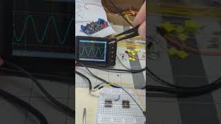
What Crossover Distortion Looks Like
On an oscilloscope, crossover distortion appears as a notch or flat spot in the output waveform at the zero-crossing point: the moment the signal transitions from positive to negative (or vice versa). The waveform looks clean on both the positive and negative halves but has a visible glitch or dead zone in the middle.
The Role of Bias Potentiometers
To eliminate this dead zone, potentiometers (bias pots) and resistors are used to apply a small standing voltage to the bases of the output transistors, keeping them slightly on at all times. In a dual-rail design, there is typically one bias pot tied to the positive rail and one tied to the negative rail.
Adjusting these pots changes how much the transistors overlap: that is, how long both the positive and negative transistors are conducting simultaneously during the crossover transition.
Setting the Bias: The Procedure
The goal is to find the point where:
- The output waveform is clean and continuous through the zero-crossing: no notch, flat spot, or discontinuity visible on an oscilloscope
- The positive and negative halves of the waveform are symmetrical: equal amplitude on both sides
- There is a controlled overlap region where both transistor pairs are conducting simultaneously, ensuring a smooth handoff Too little bias (under-biased): The crossover notch remains visible. The output waveform has a dead zone at the zero-crossing. This produces audible distortion, particularly on low-level signals and at high frequencies.
Too much bias (over-biased): The transistors conduct heavily even with no signal. Idle current is excessive, the amplifier runs very hot, and efficiency drops significantly toward Class A operation.
Correct bias: The waveform is smooth and continuous. A typical target is approximately 60% overlap, meaning both transistor pairs are conducting together for roughly 60% of the crossover transition, providing a clean handoff without excessive idle dissipation.
Practical Adjustment
With an oscilloscope connected to the amplifier output and a test signal applied:
- Start with both bias pots at minimum (transistors barely on)
- Slowly increase the positive-side bias pot while watching the waveform: the positive half of the signal will begin to clean up
- Repeat for the negative-side pot
- Adjust both pots until the zero-crossing is smooth and the waveform is symmetrical
- Verify that the amplifier is not running excessively hot at idle: some warmth is normal, but the heatsink should not become too hot to touch within a few minutes of idle operation
Efficiency Characteristics
Class A/B amplifiers are less efficient than Class D designs but more efficient than pure Class A:
| Class | Typical Efficiency | Crossover Distortion | Idle Current |
|---|---|---|---|
| Class A | ~25% | None | Very high |
| Class A/B | ~50-70% | None (when biased correctly) | Low to moderate |
| Class B | ~78% | Present | Very low |
| Class D | ~85-95% | N/A (switching topology) | Very low |
The efficiency penalty of Class A/B compared to Class D means more heat is generated per watt of output power, which is why heatsinking and thermal management are important in Class A/B designs.
Related Videos
Key Takeaways
| Characteristic | Class A/B |
|---|---|
| Output topology | Complementary push-pull transistor pair |
| Voltage supply | Dual rail (positive + negative) |
| Signal handling | NPN for positive half-cycle, PNP for negative half-cycle |
| Crossover distortion | Minimized by small quiescent bias current |
| Theoretical max efficiency | ~50% |
| Idle heat dissipation | Yes, current flows even with no signal |
| Common application | Car audio amplifiers, home stereo amplifiers |